


Compa
Compa Family CPLDs use mature processes and independent IP architecture to meet the requirements of low-power, low-cost and low-space design. It is suitable for system configuration, interface expansion and bridging, board-level power management, power-up timing management, sensor fusion and other application requirements, and can be widely used in fields such as Communications, Consumer, and Industrial Control applications.

Product Features
-
 01Logic units1K-10K LUT4 logic units, supports 3.3/2.5 V kernel or 1.2 V low-voltage kernel
 -
 02Rich interfacesSupports MIPI, LVDS, I2C, SPI, OSC, RAM, PLL etc.
 -
 03Supports RAMSupports RAM soft error detection and correction
 -
 04Supports Dual Boot functionSupports Dual Boot function with no need for Flash plugin
 -
 05High level of securitySupports functions such as background updates and disabling readback with a high level of security
 -
 06User I/OsUp to 384 user I/Os

Product Selection Guide
| Device Number1 | PGC1K | PGC2K | PGC4K | PGC7K | PGC10K | ||
| Logic resources | LUT4 equivalent | 1276 | 2428 | 4761 | 7104 | 9907 | |
| Flip-Flops | 1596 | 3036 | 5952 | 8880 | 12384 | ||
| RAM resources | Distributed RAM(Kbit) | 11 | 16 | 39 | 56 | 78 | |
| Embedded 9K block RAM | 7 | 8 | 11 | 26 | 45 | ||
| Memory blocks(Kbit) | 63 | 72 | 99 | 234 | 405 | ||
| Flash resources | Maximum embedded Flash capacity available to users(Kbits)2 | 350 | 80 | 1520 | 2070 | 3016 | |
| Clock resources | Phase Locked Loop (PLL)/Global Clock | 1/16 | 2/16 | 2/16 | 2/16 | 2/16 | |
| I/O resources | IO Banks | 4 | 6 | 6 | 6 | 6 | |
| Maximum user I/Os | 207 | 207 | 280 | 336 | 384 | ||
| Maximum differential pairs | 14 | 14 | 18 | 21 | 24 | ||
| Hard core resources | I2C hard core | 2 | 2 | 2 | 2 | 2 | |
| SPI hard core | 1 | 1 | 1 | 1 | 1 | ||
| Timer/counter hard core | 1 | 1 | 1 | 1 | 1 | ||
| On-chip oscillator | 1 | 1 | 1 | 1 | 1 | ||
| Power-up initiation time (ms) | 2.264 | 2.264 | 3 | 4.67 | 7.3 | ||
| Package | Dimensions(mm) | Ball Pitch(mm) | User I/O / Differential pairs | ||||
| UWG364 | 2.5 x 2.5 | 0.4 | 29/33 | ||||
| UWG49 | 3.2 x 3.2 | 0.4 | 39/5 | ||||
| UWG81 | 3.8 x 3.8 | 0.4 | 64/10 | ||||
| SSBG256 | 9 x 9 | 0.5 | 207/14 | 207/14 | |||
| LPG100 | 14 x 14 | 0.5 | 80/4 | 80/4 | |||
| LPG144 | 20 x 20 | 0.5 | 112/4 | 112/4 | 115/9 | 115/9 | |
| MBG256 | 14 x 14 | 0.8 | 207/14 | 207/14 | 207/18 | 207/19 | |
| FBG256 | 17 x 17 | 1 | 207/14 | 207/14 | 207/18 | ||
| MBG324 | 15 x 15 | 0.8 | 280/18 | ||||
| MBG400 | 17 x 17 | 0.8 | 336/21 | ||||
| MBG484 | 19 x 19 | 0.8 | 384/24 | ||||
| Notes: 1、PGC1K/PGC2K support version G (General) and version L (Low-Power) devices; PGC4K supports version L and version D (Dual Boot function) devices; PGC7K/PGC10K support version D devices. 2、Remaining maximum Flash capacity when not using the Dual Boot function. 3、29/3 indicates 29 user I/Os and 3 pairs of true differential output pins; the other numbers follow the same pattern. 4、UWG and SSBG packages are only available in the 1.2 V low-voltage version. |
|||||||
Technical Documentation
-
 PK03028_PGC4KLS_SBG81_V1.0
 2024.03.22
-
PK03026_PGC10KD_MBG484_V1.0 2024.03.22
-
PK03023_PGC4KL_UWG81_V1.2 2024.03.22
-
PK03015_PGC4KD_FBG256_V1.2 2024.03.22
-
PK03011_PGC7KD_MBG400_V1.2 2024.03.22
-
PK03009_PGC1KL_UWG36_V1.3 2024.03.22
-
PK03005_PGC1KG_FBG256_V1.7 2024.03.22
-
PK03003_PGC2KL_UWG49_V1.8 2024.03.22
-
UG030009_Compa Family PCB Design User Guide_V1.1 2024.03.22
-
UG030008_Compa Family GTP User Guide_V1.2 2024.03.22
-
UG030007_Compa Family CPLDs Embedded Hard Core User Guide_V1.3 2024.03.22
-
UG030006_Compa Family CPLDs Embedded Flash (EFlash) User Guide_V1.2 2024.03.22
-
UG030005_Compa Family CPLDs Input Output Interface (IO) User Guide_V1.3 2024.03.22
-
UG030004_Compa Family CPLDs Configuration User Guide_V1.7 2024.03.22
-
UG030003_Compa Family CPLDs Clock Resources User Guide_V1.4 2024.03.22
-
UG030002 Compa Family CPLDs Dedicated RAM Module (DRM) User Guide_1.2 2024.03.22
-
UG030001 Compa Family CPLDs Configurable Logic Module (CLM) User Guide_1.3 2024.03.22

Development Boards and Kits
-
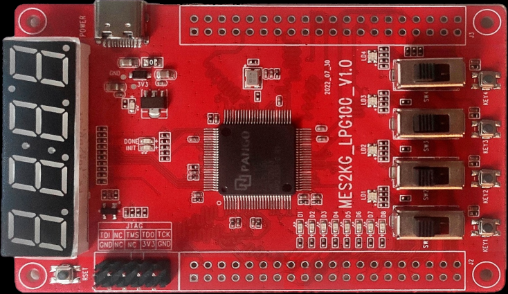
 Entry-level FPGA/CPLD learning and evaluation platformSuitable for teaching courses such as "Digital Logic Circuits," "Digital System Design and Special FPGA Lab" and "Principles and Applications of Programmable Logic Devices"Learn more
 -
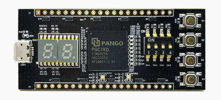
 PGC1KG/PGC2KG development board (Pango 1K/2K)1x Type-C port (power supply interface),1x JTAG interface (debugging interface)Learn more


- Products Titan Family Logos Family Compa Family Pango Design Suite
- Solutions Communication Industrial Image&Video Consumer Auto Data center Other
- Resource Software and license IP Partners
- About us Company profile Contact us Announcement
-
Contact us
86-755-66886188
[email protected]
No. 15, Gaoxin South Road,
High-Tech Industrial Park,
Nanshan District, Shenzhen
 Official public account

©2023 All Rights Reserved Shenzhen Pango Microsystems Co., Ltd. Guangdong ICP Filing No. 14029535
