


Logos-2
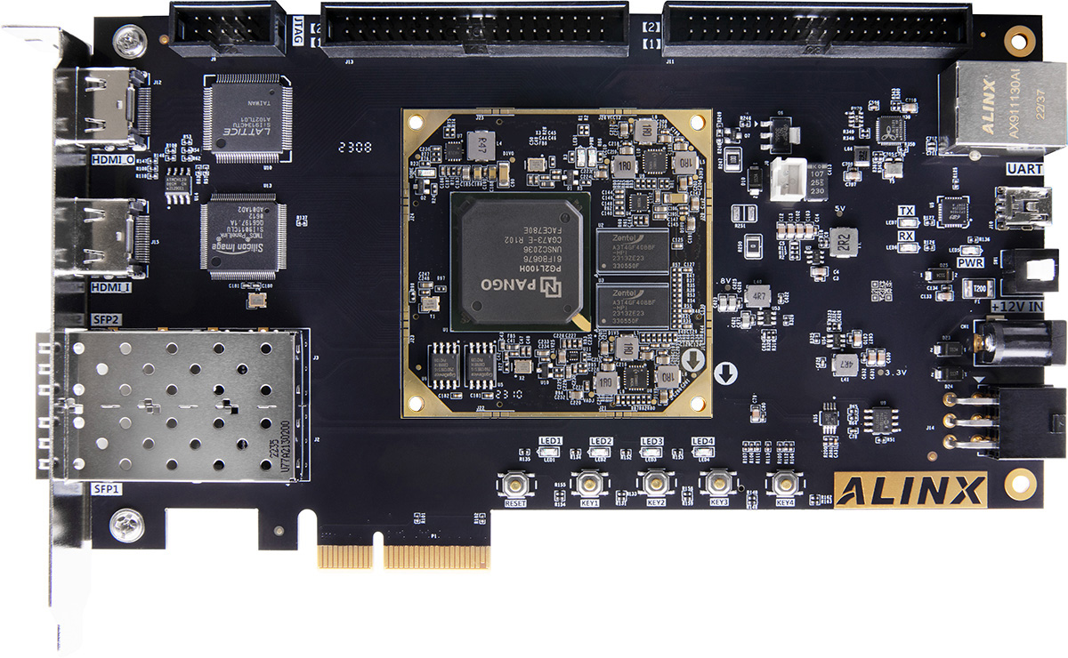
Logos-2 Family FPGAs use advanced 28nm CMOS process. It supports rich on-chip resources and high-performance interface like SerDes, DDR3, and PCIe, providing high-performance programmable solution for customers. Logos-2 is widely used in Communication, Video Processing, Data analysis, Network security, and Measurements.

Product Features
-
 01Logic resource25K~200K LUTs, flexible CLM, each CLM contains 4 LUT6 and 8 Flip-flop
 -
 02High speed memory interfaceDDR3 up to 1066Mbps
 -
 03Flexible IOSupports LVDS, TMDS, etc. LVDS up to 1.25Gbps
 -
 04Internal RAMSoft error detection and correction supported
 -
 05ADC hardcoreResolution12 bit, sampling rate 1MSPS
 -
 06AES encryptionAdvanced 256-bit AES encryption

Product Selection Guide
| Part Number | PG2L25H | PG2L50H | PG2L100H | PG2L100HX3 | PG2L200H | ||
| Logic elements | LUT4 equivalent | 26700 | 53700 | 99900 | 99900 | 239700 | |
| Flip-Flops | 35600 | 71600 | 133200 | 133200 | 319600 | ||
| RAM resources | Distributed RAM (Kbit) | 344 | 594 | 1244 | 1244 | 2469 | |
| Block RAM (36Kbit each) | 55 | 85 | 155 | 155 | 415 | ||
| Total block RAM (Kbit) | 1980 | 3060 | 5580 | 5580 | 14940 | ||
| Clock resources | GPLL+PPLL | 3+3 | 5+5 | 6+6 | 6+6 | 10+10 | |
| IO resources | Max. user I/O | 150 | 250 | 300 | 300 | 500 | |
| Max. differential I/O(pairs) | 72 | 120 | 144 | 144 | 240 | ||
| DDR3(Mbps) | 1066 | 1066 | 1066 | 1066 | 1066 | ||
| Hard core resources | APM(25*18) | 80 | 120 | 240 | 240 | 740 | |
| ADC hard cores | 1 | 1 | 1 | 1 | 1 | ||
| PCIe Gen2x4 | 1 | 1 | 1 | 1 | 1 | ||
| AES module blocks | 1 | 1 | 1 | 1 | 1 | ||
| HSST(6.6Gbps) | 4 | 4 | 8 | 8 | 16 | ||
| Package | Dimensions(mm) | Ball Pitch(mm) | User I/O /HSST | ||||
| MBG324 | 15 x 15 | 0.8 | 210/0 | 210/0 | 210/0 | ||
| MBG325 | 15 x 15 | 0.8 | 150/4 | ||||
| FBG4841 | 23 x 23 | 1 | 250/4 | 285/4 | 285/4 | ||
| FBB4841 | 23 x 23 | 1 | 285/4 | ||||
| FBG6762 | 27 x 27 | 1 | 300/8 | 300/8 | |||
| FBB6762 | 27 x 27 | 1 | 400/8 | ||||
| FFBG1156 | 35 x 35 | 1 | 500/16 | ||||
| Note: 1、FBG484 and FBB484 pin to pin compatible 2、FBG676 and FBB676 pin to pin compatible 3、PG2L100HX supports 1.25Gbps high-speed LVDS |
|||||||
Technical Documentation
-
 PK04001_PG2L100H_FBG676_V1
 2024.10.17
-
PK04002_PG2L100H_MBG324_V1 2024.10.17
-
PK04003_PG2L100H_FBG484_V1.2 2024.10.17
-
PK04004_PG2L25H_MBG325_V1.1 2024.10.17
-
PK04005_PG2L50H_FBG484_V1.1 2024.10.17
-
PK04006_PG2L50H_MBG324_V1.1 2024.10.17
-
PK04007_PG2L200H_FFBG1156_V1.0 2024.10.17
-
PK04008_PG2L200H_FBB676_V1.0 2024.10.17
-
PK04009_PG2L200H_FBB484_V1.0 2024.10.17
-
UG040001_Logos2 Family FPGAs Configurable Logic Module (CLM) User Guide_V1.4 2024.10.17
-
UG040002_Logos2 Family FPGA Dedicated RAM Module (DRM) User Guide_V1.2 2024.10.17
-
UG040003_Logos2 Family FPGA Arithmetic Process Module (APM) User Guide_V1.3 2024.10.17
-
UG040004 Logos2 Family FPGAs Clock Resources (Clock) User Guide_V1.2 2024.10.17
-
UG040005_Logos2 Family FPGA Configuration User Guide_V1.3 2024.10.17
-
UG040006_Logos2 Family FPGA InputOutput Interface (IO) User Guide_V1.2 2024.10.17
-
UG040007_Logos2 Family Product GTPs User Guide_V1.2 2024.10.17
-
UG040008_Logos2 Family FPGAs High-Speed Serial Transceiver (HSSTLP) User Guide_V1.9 2024.10.17
-
UG040009_Logos2 Family FPGAs Analog-to-Digital Converter (ADC) ModuleUser Guide_V1.6 2024.10.17
-
UG040012_Logos2 Family Hardware Design Guide_V1.4 2024.10.17


- Products Titan Family Logos Family Compa Family Pango Design Suite
- Solutions Communication Industrial Image&Video Consumer Auto Data center Other
- Resource Software and license IP Partners
- About us Company profile Contact us Announcement
-
Contact us
86-755-66886188
[email protected]
No. 15, Gaoxin South Road,
High-Tech Industrial Park,
Nanshan District, Shenzhen
 Official public account

©2023 All Rights Reserved Shenzhen Pango Microsystems Co., Ltd. Guangdong ICP Filing No. 14029535
